The most recent socket. Processor sockets, what is a processor socket
The sockets of any processors originate from the socket for microcircuits, being, in fact, microcircuits for the logical execution of program codes. The first processors were no different in design from other microelectronic devices and at first did not have a socket for installation and were soldered directly onto a printed circuit board, also known as - motherboard.
Let's look at all the Intel processors created today and the sockets for them that went into production:
History of sockets before the creation of mass personal computers
Socket DIP– had a standard design for a 40-pin microcircuit design, suitable not only for early models of Intel processors, but also for various microcircuits of that time. Used by eight-bit Intel processors since 1970 8008 , 8080 And 8085 . Speed characteristics – 5-10 MHz. PLCC socket– its use began around 1978, the socket became the prototype of all executable sockets for processors. The socket is made in the form of a recessed square, the sockets of the processor legs are made along the edges of the socket. Used by 32-bit series processors 80186 , 80286 , 80386 since 1982. Speed characteristics – 6-40 MHz.The first personal computers
Socket 1– with the release of this socket in 1989, the era of processors made in PGA form factor. The socket had a square design with sockets for numerous processor legs. The processors had 169 pins with motherboard and were the first mass-produced processors personal computers. The socket was used by series processors 80486DX, 80486GX, 80486SX, 80486SL, 80486DX2, 80486DX4. Speed characteristics – 16-33 MHz.Socket 2– was a continuation of the development of sockets for processors. The socket was used at the same time as Socket 1, but had more contacts - 238. Processors were used from the same series, speed characteristics increased - 25-83 MHz.
Socket 3– created for interfacing processors based on the 486 series of processors. The socket is also used by AMD 486 series processors, the speed characteristics do not change 25-83 MHz.
The first computers worldwide
Socket 4– the first socket for series processors Pentium 1, supported overclocking and replacement functions, the processors operated on a bus from 60 to 66 MHz, which accordingly made it possible for the first Pentiums to have speed characteristics of 120-133 MHz. Supported installation of 273-pin processors since 1993.Socket 5– continued the development of Intel processors and was made to operate on a system bus from 50 to 66 MHz, and supported the installation of 320-pin processors Intel Pentium 1. Processors were also produced for it third party developers. We can say that this was the first standard socket for processors up to 300 MHz.
Socket 6- slightly modified Socket 3, due to its late release for the 486 series processors, is poorly known on the market. It had a 235-pin processor socket. Speed characteristics up to 166 MHz.
The first fully multimedia computers
Socket 7– the most common socket for all processors up to 300 MHz, meaning that based on the terminology of Intel Pentium 1, it ended with the use of fifth-generation technology at 300 MHz. It had a design with 321 contacts. Supported processors Pentium MMX And Intel Pentium, and third-party processors. Produced since 1994.Socket 8– designed specifically for the processor Intel Pentium PRO and processor Intel Pentium 2 OverDrive, had 387 pin sockets for the processor and was made in a rectangular form factor. The speed characteristics of the processors used are up to 333 MHz. Released in 1995, the socket was discontinued in favor of the Slot 1 connector. Socket SLOT 1– to use all processor capabilities Intel Pentium II and further Intel Pentium 3, the main feature is an increased processor cache, removed from the processor core; processors are created that are implemented on printed circuit board with 242 edge contacts, different contact name SC242. Start of connector production in 1997. Supported processors Intel Pentium 2 And Intel Pentium III, as well as third-party processors. An adapter for processors was released Socket 370, the processors were inserted into an adapter, which in turn was connected to SLOT 1. Speed characteristics from 233 to 1200 MHz. SLOT 2 connector– designed for server and multitasking solutions using Intel Pentium 2 and Intel Pentium 3 Xeon series, unlike SLOT 1 it supported a second cache level of up to 2 Megabytes. Somewhat vaguely reminiscent of the SLOT 1 connector but had 330 contacts. Speed characteristics from 400 to 100 MHz.
The era of modern computers
Socket 370– the most common socket for Intel processors. This is where the era of dividing Intel processors into inexpensive solutions begins Celeron with trimmed cache and Pentium– more expensive full versions of the company’s product. The connector was installed on motherboards with a system bus from 60 to 133 MHz. The socket is made in the form of a square plastic movable box; when installing a processor with 370 contacts, a special plastic lever presses the processor legs to the connector contacts. Supported processors Intel Celeron Coppermine, Intel Celeron Tualatin, Intel Celeron Mendocino, Intel Pentium Tualatin, Intel Pentium Coppermine. Speed characteristics of installed processors range from 300 to 1400 MHz. Supported third party processors. Produced since 1999.Socket 423– first socket for processors Pentium 4. It had a 423-pin grid of legs and was used on motherboards of personal computers. It existed for less than a year, due to the inability of the processor to further increase in frequency, the processor could not pass the frequency of 2 GHz. Replaced by Socket 478 connector. Production began in 2000.
Socket 478– released to follow the competitor’s connector (AMD) Socket A, since previous processors were unable to raise the 2 Gigahertz bar, and AMD took the lead in the processor manufacturing market. The connector supports Intel solutions - Intel Pentium 4, Intel Celeron, Celeron D, Intel Pentium 4 Extreme Edition. Speed characteristics from 1400 MHz to 3.4 GHz. Produced since 2000. Socket 495– connector for mobile solutions from Intel. It had 495 contacts and supported the Intel Celeron series of processors. Speed characteristics 450 – 900 MHz. Produced since 2000.
PAC418 socket– special socket for pairing processors Intel Itanium made using IA-64 technology and were server processors supplied to HP and a number of other companies. It was carried out on a printed circuit board and had, accordingly, 418 edge contacts. Speed characteristics up to 800 MHz. Produced since 2001.
Socket 603– Intel's next server connector for the Xeon series. A Socket 603 processor could be installed in Socket 604. Made in a square form factor, it had 603 slots for processor legs. Speed characteristics of installed processors range from 1400 MHz to 3 GHz. Produced since 2001.
Socket PAC611– is a 611-pin microprocessor socket for installation on processor motherboards Intel Itanium 2. The speed characteristics of the installed processors are 800-1000 MHz. Produced since 2002.
Socket 604– intended for server platforms and workstations, a continuation of the Socket 603 connector. Made in a 604-pin design. Intended for Intel processors Xeon E7xxx series, motherboards with this socket used a bus from 400 to 1066 MHz. Produced since 2002. Speed characteristics from 1600 MHz to 3800 MHz. Socket 479- intended for use in mobile solutions, has 479 pin sockets for Intel processors. Although the purpose was mobile computers, it was used in desktop solutions. Pentium M processor The design for this socket had 478 contact pins. The remaining processors for this socket are: Pentium III M released in 2001, Pentium M And Celeron M version 3xxx and later compatible socket processors. Produced since 2003. Speed characteristics from 400 MHz and higher.
Today's computers
Socket 775 or Socket T– the first connector for Intel processors without sockets, made in a square form factor with protruding contacts. The processor was installed on the protruding contacts, the pressure plate was lowered, and using a lever it was pressed against the contacts. Still used in many personal computers. Designed to work with almost all fourth generation Intel processors - Pentium 4, Pentium 4 Extreme Edition, Celeron D, Pentium Dual-Core, Pentium D, Core 2 Quad, Core 2 Duo and Xeon series processors. Produced since 2004. Speed characteristics of installed processors range from 1400 MHz to 3800 MHz.Socket M– the most common mobile socket. It was used for almost all Intel mobile processors, and is still relevant in the production of laptops. Made in 478-pin design. Designed for Intel processors - Celeron, Core Solo, Core 2 Duo, Core Duo , Celeron M. Produced since 2006. Speed characteristics of processors from 1600 MHz to 3000 MHz.
Socket J or socket LGA 771– the server socket, updated in 2006, has a design with protruding contacts. Intended for server solutions. The socket is used by such Intel processors - Dual-Core And Quad-Core Xeon series, Core 2 Extreme QX9775. Speed characteristics from 2 GHz and higher.
Socket P– a modern socket for mobile processors. Has 478 contact sockets. Produced since 2007. Designed for all Intel mobile processors - Dual-Core with T5xxx By T9xxx, Penium Dual-Core with Т23хх By T4xxx, Core 2 Quad. Speed characteristics from 1.6 GHz and higher.
Socket 441– a special socket designed for processors Intel Atom . Used only for these low-power processors. Produced since 2008. Speed characteristics from 600 MHz to 2100 MHz. LGA 1366 socket– one of the main connectors from Intel on this moment. Made in 1366 contact form, produced since 2008. Supports Intel processors – Core i7 series 9xx, Xeon series 35xx to 56xx, Celeron P1053. Speed characteristics from 1600 MHz to 3500 MHz.
LGA 1156 socket– the most modern Intel socket today. Made using 1156 protruding contacts. Produced from 2009 to this day. Designed for modern Intel processors for personal computers. Speed characteristics from 2.1 GHz and higher.
LGA 1248 socket– designed for processors Intel Itanium 93xx series, performed for server solutions and workstations. Start of technology support Intel QuickPath. Produced since 2010. Has 1248 protruding contacts for interface with the processor. Speed characteristics – up to 19 GB/s.
LGA 1567 socket– designed for server rooms Xeon processors series 75xx and 76xx. Made in 1567 contact version, produced since 2010. Speed characteristics from 19 GB/s to 25.6 GB/s.
Near future
LGA 1155 socket or Socket H2– intended to replace LGA socket 1156. Supports the latest processor Sandy Bridge and future Ivy Bridge. The connector is made in 1155-pin design. Produced since 2011. Speed characteristics up to 20 GB/s. LGA 2011 socket or Socket R– the latest development from Intel, will replace LGA 1366. The connector is made in a 2011-pin design. Supports Sandy Bridge E-series processor. New processors are currently being developed for the socket. Speed characteristics from 19 GB/s to 25.6 GB/s.During the upgrade process or when configuring a new system unit, one of the main factors for its successful assembly is the correctly selected and compatible components. To achieve this, manufacturers have introduced certain standards for the compatibility of these same components.
For example, when replacing a central processor, there is a different designation (CPU), it is very important to understand exactly what type of socket it has and whether it will fit the connector on the motherboard of a personal computer.
What it is
 Basic and very important parameter motherboards - central processor socket (CPU socket). This is a socket located on the main board of the computer, intended for installing a CPU into it. And before connecting these components into one coherent system, you need to determine whether they are compatible with each other or not. It's like plugging a plug into a socket., if the plug is American standard and the socket is European, then naturally they will not fit together and the device will not work.
As a rule, in retail outlets selling computer components, in the price tag on the window or in the price list, the main parameters of the processor that is being sold are always indicated. Among these parameters, the type of socket to which it is suitable is indicated. this processor. The main thing when buying is to take into account this primary characteristic of the CPU.
This is important because when installing the processor into the motherboard socket, when wrong choice socket it simply won’t fit into its place. In existing today huge selection connectors are divided into two main types:
- Sockets for central processors from the manufacturer AMD.
- Sockets designed for processors manufactured by Intel.
Intel and AMD socket specifications
- Physical dimensions of socket.
- The method of connecting the contacts of the socket and the processor.
- Type of mounting of the CPU cooler cooling system.
- The number of sockets or contact pads.
 Connection method - there is nothing complicated here. The socket has either sockets (like AMD) into which the processor contacts are inserted. Either pins(like Intel), on which the flat contact pads of the CPU rest. There is no third option here.
The number of sockets or pins - there are many options here, their number can range from 400 to 2000, and maybe even more. You can determine this parameter by looking at the marking of the socket, in the name of which is encoded this information. For example, the Intel Core i7-2600 for the Intel LGA 1155 processor socket has exactly 1155 contact pads on its surface. The abbreviation LGA means that the processor has flat contacts, and the socket, on the contrary, consists of 1155 pins.
Well, the mounting methods for the CPU cooling system may differ: in the distance between the holes on the motherboard designed to secure the lower part of the cooling system. And the method of fixing the upper half, consisting of a radiator and cooler. There are also exotic cooling options made at home, or systems with a water method of lowering the CPU temperature.
There are other characteristics that are directly related to the functionality of the entire motherboard and its performance. The presence of a socket of a certain standard also indicates what possible parameters are included in this platform and how modern this motherboard is. Here are some features that distinguish a board built on a specific socket and a chipset developed for it:
- Processor clock speed range, number of supported cores and data transfer speed.
- The presence of controllers on the motherboard that expand the functionality of the board.
- Support or presence of a built-in graphics adapter in the motherboard or main processor.
How to determine the socket of a processor
The main component that performs the main task in the operation of a computer is the CPU. And if it fails, then there is nothing left to do but replace it with an analogue similar in connector and characteristics . This is where the challenge arises by determining the socket type. There are many options to find out, and here are three main and available ones.
By manufacturer and model
An easy method using access to World Wide Web(i.e., via the Internet). All the necessary data on products produced by a particular motherboard manufacturing company is available on the manufacturers’ official websites. The information is not hidden anywhere and can be studied by anyone. You just have to hit it search bar the data needed for this.
Here is an approximate sequence of actions:

Via Speccy
- Download and install the Aida64 or Speccy application on your computer. Next, let's consider the second option. Open the Speccy program. And find in it the section with CPU parameters, it should be called “Central Processor”.
- Next, in the selected section, find the line called “Constructive” and read its contents. This is where the type of processor socket will be indicated.
- Approximately the same steps will need to be performed when using the Aida64 program. Section “Computer”, subsection DMI, then in the subsection “Processor”, look for a line with the word Socket.
In the documentation
 This method is the easiest, but requires documentation attached to the system unit upon purchase. Among the many instructions for the motherboard, processor, video adapter and other components from which the computer is assembled, those intended for the CPU and motherboard are suitable. Carefully scroll through the entire manual and look in it for the words: connector, socket type. This is where information about the socket standard of the motherboard or processor should be.
A personal computer is not a cheap thing, and in some versions it can even cost as much as an old used car. And change it very often- it's a pretty unprofitable business. Even reputable and successful companies do this relatively rarely. But, despite this, from time to time you still have to upgrade and speed up the computing capabilities of any computer.
To do this, you have to disassemble the old hardware and find out information about certain characteristics and parameters. However, you need to take into account your abilities for such procedures. Here, as people say: “If you can’t, don’t bother.” And if there is uncertainty about the success of such an event, then it is better to contact special service centers or to individual experienced craftsmen.
A socket is a processor socket developed by Intel and made using Land Grid Array (LGA) technology. It is a connector with spring-loaded or soft contacts, to which a processor that does not have pin contacts is pressed using a special holder with a grip and a lever. The increase in the number of its contact pads is associated with the transfer of North Bridge components directly to the processor chip.
Socket LGA 775
Socket LGA 775 (or Socket T) is one of the most common sockets for Intel processors at the moment (Fig. 1). It is a connector with spring-loaded (or soft) contacts, to which a processor that does not have pin contacts is pressed using a special holder with a grip and a lever.
Socket T (LGA 775) defines following parameters motherboard computer:
Processor socket type - LGA;
Processor form factor - Flip-chip land grid array;
Number of contacts - 775;
The bus used is Quad-Pumped FSB;
FSB frequency, MP/s - 533, 800, 1066, 1333 or 1600;
Processor size - 37.5 × 37.5 mm;
Connectable processors: Intel Pentium 4 (2.66 - 3.80 GHz), Intel Celeron D (2.53 - 3.6 GHz), Pentium 4 Extreme Edition (3.20 - 3.73 GHz), Pentium D (2 ,66 - 3.60 GHz), Pentium Extreme Edition (3.20 - 3.73 GHz), Pentium Dual-Core (1.40 - 2.80 GHz), Core 2 Duo (Exxxx, except 6x05 and 8x35), Core 2 Extreme (X6800; Qхxxxx, except 9775 and 9300), Core 2 Quad (Qxxxx, except 9000 and 9100), Xeon (1.86 - 3.00 GHz), "Core" Celeron (1.60 - 2.00 GHz).
This connector uses a bus that is less efficient than that of AMD, but unlike the bus AMD Athlon it is scalable. Since the Pentium 4 and Core 2 Duo processors do not contain a memory controller, this allowed Intel to use the old bus with more high frequency. However, memory and cache efficiency (all other things being equal) is slightly lower than that of AMD processors. When switching to new FB-DIMM memory, Intel planned to abandon or significantly modify this connector. However, the high power consumption of this memory forced us to reconsider the decision in favor of DDR3 and further development of this direction.
Socket LGA 1366 (Socket B)
Socket LGA 1366 (or Socket B) is the successor to the LGA775 processor socket for high-end desktop systems and the LGA 771 processor socket for servers from Intel. Socket LGA 1366 (Fig. 2) defines the following parameters of the computer motherboard:
Processor socket type - LGA;
Processor form factor: Flip-chip land grid array;
Number of contacts: 1366;
Buses used: 3 DDR3 channels (the memory controller in the Core i7 9xx supports up to 3 memory channels, and each can have one or two DDR3 DIMMs, so motherboards on the LGA 1366 socket support up to 6 memory sticks, not 4 , like Core 2); 1 or 2 QPI connections (each 4.8 - 6.4 GPU/s);
Voltage, V: 0.75 - 1.375;
Processor size: 45 mm × 42.5 mm;
Processor family: Intel Core i7 (9xx), Intel Xeon - LC,EC,W (35xx), W (36xx), EC,LC,E,L,X (55xx), E,L,X (56xx), Intel Celeron P1053; the protective cover of the processors consists of nickel-plated copper, the substrate is silicon, and the contacts are made of gold-plated copper;
The minimum and maximum storage temperatures for Core i7 are: − 55 °C and 125 °C;
The maximum heat dissipation of Core i7 processors is 130 W, in idle mode it is 12-15 W, the efficiency of a standard Core i7 cooler decreases sharply if the temperature inside the system unit exceeds 40 °C.
More details about supported processors:
- JasperForest: Intel Celeron P1053 - 1.33 GHz, 1 core (2 threads, 256 KB L2, 2 MB L3), 3* DDR3-800 (with ECC support), 30 W;
- Gulftown: Core i7 970 - 3.20 GHz (Turbo Boost - 3.46 GHz), TDP 130 W, Core i7 980X - 3.33 GHz (Turbo Boost - 3.6 GHz), TDP 130 W;
- Bloomfield: Core i7 960 - 3.20 GHz (4x256 KB L2, 8 MB L3), Core i7 950 - 3.06 GHz (4x256 KB L2, 8 MB L3), Core i7 940 - 2.93 GHz (4x256 KB L2, 8 MB L3), Core i7 930 - 2.80 GHz (4x256 KB L2, 8 MB L3), Core i7 920 - 2.66 GHz (4x256 KB L2, 8 MB L3), Core i7 965 Extreme Edition - 3.2 GHz (4x256 KB L2, 8 MB L3), Core i7 975 Extreme Edition - 3.33 GHz (4x256 KB L2, 8 MB L3) and Xeon 55xx series.
Supports work with the updated voltage stabilizer module - Voltage Regulator Module 11.1. The latter supports a number of new features such as Power on Configuration (POC), Market Segment Identification (MSID) and Power State Indicator Input (PSI#). The VID_Select, VR-Fan and VR10 VID functions have been removed from VRM 11.1. The increase in the number of contact pads is due to the transfer of the memory controller directly to the processor chip and the use of the new QuickPath Interconnect protocol instead of the previously used Quad-Pumped Bus.
Since processors for the LGA 1366 socket have the FSB replaced with QPI (QuickPath Interconnect), this means that the motherboard must use a chipset that supports QuickPath Interconnect (in 2012 this technology was already supported Intel chipsets X58 and Intel X79).
Socket LGA 1356 (Socket B2)
Socket B2, also known as LGA 1356 processor socket, compatible with processors Intel Sandy Bridge. LGA 1356 is designed as a replacement for LGA 1366 (Socket B). It is a connector with 1356 spring-loaded contacts. LGA 1356 and LGA 1366 processors are not compatible with each other, since they have different slot locations (the main difference between LGA 2011 and LGA 1356 is the number of QPI buses: on LGA 2011 there are two, and on LGA 1356 there is only one QPI bus, except In addition, LGA 2011 has two additional PCI-E 3.0 lanes, as well as support for a fourth DDR3 channel).
Socket LGA 1356:
Processor form factor: Flip-chip, LGA;
Number of LGA 1356 pins: 1356;
Buses used: 3 channels DDR3, QPI, DMI;
Processors: Intel Sandy Bridge.
Processors:
Skylake-U (BGA 1356) - for mobile devices (ultrabooks, thin and light laptops);
Skylake-H (BGA 1440) - high-performance laptops;
Skylake-Y (BGA 1515) - fanless devices, tablets and hybrid gadgets.
Socket LGA 1156 (or Socket H)
Socket H (or LGA 1156) is the successor to the LGA 775 processor socket for desktop systems and the LGA 771 processor socket for mid- and entry-level servers from Intel (Fig. 3). It is an alternative to the more expensive platform based on the X58 chipset and the LGA 1366 socket. LGA 1156 provides support for processors with an integrated graphics adapter. Currently for this processor socket processors of the Core i3, i5 and i7 8XX families are produced, as well as cheap processors under the Pentium brand.
Socket LGA 1156 (Fig. 3) defines the following parameters of the computer motherboard:
Connector type: LGA;
Processor form factor: Flip-chip land grid array;
Number of contacts: 1156;
Buses used: 2 channels DDR3, DMI, PCIe 16x;
Processors: Intel Core i7 (8xx), Intel Core i5 (7xx, 6xx), Intel Core i3 (5xx), Intel Pentium G69x0, Intel Celeron G1101, Intel Xeon X,L (34xx).
LGA 1156, unlike LGA 1366, is connected to the chipset via DMI directly, instead of QPI and north bridge. It has two memory channels instead of three and a PCI-Express 2.0 x16 connection. Chipsets for motherboards with LGA 1156 are produced by Intel, including products for servers - 3400, 3420, 3450; for desktop machines - P55, H55, H57, Q57 (only the last three support video built into the processor). The P55 chipset was introduced first, and therefore, if the board was released before the Core i3, Core i5 6xx entered the market, then to use them you will need to update the BIOS (all chipsets and processors are at least partially compatible with each other, for example: on a board with P55 you can install a Clarkdale processor, but its video core will remain unused, and on H/Q (55/57) you can install a Lynnfield processor, but the video outputs will also remain unused, and many server boards are equipped with third-party video).
Socket LGA 1155 (Socket H2)
Socket LGA 1155 is a processor socket for Intel Sandy Bridge processors, designed as a replacement for LGA 1156 (Socket H). Despite their similar design, LGA 1155 and LGA 1156 processors are incompatible with each other and have different slot locations. Cooling systems with mount for LGA 1156 are compatible with LGA 1155, which allows you to avoid purchasing new system cooling for new processors.
An important difference between LGA 1155 processors and chipsets compared to LGA 1156 analogues is the twice faster version of the DMI bus, which connects the processor to the chipset, which eliminates the bottleneck when using SATA 6Gb/s and USB3.0 controllers, and also supports processors with an integrated graphics adapter (in the future, processors with up to eight cores will be released for this socket). Socket LGA 1155 (Fig. 4) defines the following parameters of the computer motherboard:
Number of contacts: 1155;
Buses used: 2 channels DDR3, DMI, PCIe 2.0 16x;
Processor size: 37.5 × 37.5 mm;
Processors: Intel Sandy Bridge, Intel Ivy Bridge.
Chipsets Q65, B65, H61, Q67, H67, P67, Z68, B75, Q75, Q77, H77, Z75, Z77.
ProcessorsSandyBridge.Chipsets (Tables 2, 3) for Sandy Bridge (except Q65, Q67 and B65) will support both Sandy Bridge and Ivy Bridge processors (even without forced BIOS updates). Systems based on Sandy Bridge processors officially support memory up to DDR3-1333, but in practice they successfully worked with memory at speeds up to DDR3-2133. USB 3.0 is not supported by any chipset (motherboard manufacturers provide support for USB3.0 using third-party chips).
ProcessorsIvyBridge. All motherboards with Ivy Bridge chipsets support both Ivy Bridge and Sandy Bridge processors. Processors of the Ivy Bridge family initially officially support RAM up to DDR3-1600, while Sandy Bridge only up to DDR3-1333. Owners of Ivy Bridge chipsets can also use overclocking for K-series processors.
Socket LGA 2011(Socket R)
LGA 2011, also known as Socket R, is a socket for Intel processors that is expected to supplant LGA 1366 (Socket B) in high-end desktop systems.
The LGA 2011 platform (for Sandy Bridge-E) is positioned by Intel as a solution for creating PCs with the maximum level of performance. A distinctive feature of the entire line of processors is support for a four-channel DDR3 memory subsystem (enthusiasts will have access to 4/6/8-core Sandy Bridge E processors with support for a 4-channel memory controller).
LGA 2011 processors will use the Sandy Bridge architecture, but will lose the overclocking limitations inherent in the LGA 1155 platform. The LGA 2011 platform will be able to work not only with Sandy Bridge-E generation processors, but also with their successors in the form of Ivy Bridge-E, or even later Haswell processors.
Socket LGA 2011 (Fig. 5) defines the following parameters of the computer motherboard:
Processor form factor: Flip-chip, LGA
Number of contacts: 2011
Buses used: 4 DDR3, QPI, DMI channels and 40 PCIe 3.0 lanes
Processor size: 58.5x50 mm
Processors: Intel Sandy Bridge-EX
LGA 2011 uses the QPI bus to connect to the additional processor in dual-processor systems or to additional chipsets. The processor performs north bridge functions, such as a memory controller, PCI-E bus controller, DMI, FDI, etc.
For Intel Sandy Bridge-EP server solutions, the actual differences from Sandy Bridge chips will be a larger number of processor cores (up to eight), a corresponding LGA2011 processor socket, a larger L3 cache, an increased number of DDR3 memory controllers and support for PCI-Express 3.0. The structure of the chip can be divided into the following main elements: processor cores, graphics core, L3 cache memory and the so-called “System Agent”. To increase the overall performance of the system, the developers used the ring topology of the 256-bit intercomponent bus, based on a new version of QPI (QuickPath Interconnect) technology, expanded, modified and first implemented in the architecture of the Nehalem-EX server chip (Xeon 7500), as well as planned for use in conjunction with the Larrabee chip architecture.
The ring bus is used to exchange data between six key components of the chip: x86 processor cores, graphics core, L3 cache and system agent. Ring bus performance is rated at 96 GB per second per link at 3 GHz, effectively four times faster than previous generation Intel processors. Bus management is carried out using communication protocol distributed arbitration, while pipelined processing of requests occurs at the clock frequency of the processor cores, which gives the architecture additional flexibility when overclocking. The bus consists of four 32-byte rings: the Data Ring, the Request Ring, the Snoop Ring and the Acknowledge Ring, in practice this actually allows you to share access to the 64-byte interface last level cache into two different packages.
The ring topology and bus organization ensures minimal latency when processing requests, maximum performance and excellent scalability of the technology for chip versions with different numbers of cores and other components. In the future, up to 20 processor cores per chip can be connected to the ring bus, and in addition, the ring bus is physically located directly above the L3 cache memory blocks in the upper level of metallization, which simplifies the design layout and makes the chip more compact. L3 - the last third level cache (LLC) is distributed not only between processor cores, but, thanks to the ring bus, also between the system agent.
The system agent includes a DDR3 memory controller, a power control unit (PCU), PCI-Express 2.0, DMI controllers, etc. Like all other elements of the architecture, the system agent is connected to the overall system via a high-performance ring bus.
Each processor core has direct access to its “own” L3 cache segment, with each L3 cache segment providing half the width of its bus for ring data bus access, while physical addressing of all four cache segments is provided by a single hash function. Each L3 cache segment has its own independent ring bus access controller; it is responsible for processing requests for the placement of physical addresses. In addition, the cache controller constantly communicates with the system agent to monitor failed L3 accesses, monitor intercomponent communication, and uncacheable accesses.
The power management controller located in the system agent is responsible for timely and dynamic scaling of supply voltages and clock frequencies of processor cores, caches, memory controller and interfaces. What is especially important to emphasize is power management and clock frequency produced independently for processor cores and graphics core. The new version of Turbo Boost technology is implemented not least thanks to this power management controller. Depending on the current state of the system and the complexity of the problem being solved, the Sandy Bridge microarchitecture allows Turbo Boost technology to “overclock” the processor cores to a level significantly exceeding TDP for quite a long time.
Although the location of the mounting holes for the LGA2011 and LGA1366 sockets are the same, not all “old” coolers are suitable for LGA 2011 (the LGA2011 mounting frame has threads on the holes, which may require modifications to the cooler mounting system). The maximum level of power consumption of processors within the LGA 2011 platform can be 150 W. LGA 2011 was announced along with Sandy Bridge-EX back in November 2011.
Socket LGA 1150 (or Socket H3)
Socket LGA 1150 - processor socket for Intel processors Haswell, and his successor Broadwell(beginning of release 2013/2014, respectively). LGA 1150 is designed as a replacement for LGA 1155 (Socket H2). Socket LGA 1150 defines the following parameters of the computer motherboard:
Processor form factor: Flip-chip, LGA;
Number of contacts: 1150;
Buses used: 2 channels DDR3, DMI, PCIe 3.0 x16/2x8;
Processor size: 37.5 x 37.5 mm;
Processors: Intel Haswell, Intel Broadwell.
Haswell is the code name for a processor microarchitecture being developed by Intel that is planned as a successor to Ivy Bridge. Designed for 22nm manufacturing technology based on transistors with a 3D gate structure.
Architecture Features Haswell:
Technological process - 22 nm;
Design LGA 1150;
The basic number of cores is 2 or 4;
Completely new cache design;
Improved energy saving mechanisms;
Integrated vector coprocessor possible;
Adding Advanced Vector Extensions 2 instructions, in particular FMA (Fused Multiply Add);
Extension of TSX commands (en:Transactional Synchronization Extensions) for hardware support of transactional memory;
Power consumption is 30 percent lower compared to analogues from the Sandy Bridge line (in addition, future chips will reduce the power consumption of the platform during the standby period by more than 20 times compared to existing designs without sacrificing performance);
64 MB eDRAM memory (separate chip, but common packaging).
The chip will implement the ability to simultaneously work with four operands, allowing one instruction to perform two multiplication and addition or subtraction operations at once. Haswell may also acquire a Level 4 cache, which will be used by the integrated graphics core to offset the impact of low bandwidth system memory. With the advent of Haswell, Intel plans to divide its product portfolio into two groups: desktop and mobile versions; special versions for ultrabooks. Desktop versions of the processors will be available with two or four processor cores with a TDP of 35, 45, 65 or 95 watts, a dual-channel DDR3/DDR3L memory controller, as well as integrated GT2 and GT1 graphics cores. Mobile versions will also be available in dual- or quad-core configurations, but will be equipped with a more powerful GT3 graphics core and a memory controller that only supports DDR3L DIMM. Mobile computers based on Intel Haswell will be able to work without recharging for a whole day, and in standby mode, if available, network connection this period will be more than 10 days. Among other things, Haswell processors will likely feature some performance improvements, details of which will obviously become known later. According to the tick-tock principle, a reduction in the process technology to 14 nm is expected a year after the introduction of the chip - this architecture will be called Broadwell.
In 2014, the company released a successor to the Haswell processor architecture, called Broadwell, which uses the first truly integrated system-on-a-chip (SoC) design. Compared to its predecessor, Broadwell will receive some architectural changes. In addition to the actual SoC design, the chip houses Ethernet, Thunderbolt or USB 3.0 controllers. The graphics core is also inherited from Haswell, will have support for DirectX 11.1 and image output in resolutions up to 4K. Like Haswell, the processor uses the same 947-pin pad for mobile computing and LGA 1150 for desktop computing, meaning the Intel platform is compatible with two generations of processors.
Socket LGA 1151.
Many people, when assembling a PC, or when purchasing a ready-made solution based on a particular processor, are faced with the concept of “socket”. Let's guess: half have no idea what it is or what it is intended for. In this article we will look at what this term represents, as well as the main sockets of AMD processors.
The Reds have always had a loyal policy regarding substitutions processor sockets: maximum preservation of compatibility with obsolete chips, uniform fasteners for cooling systems (AM2-AM3+ generation), easy BIOS flashing and more. But how the company’s technologies developed is the topic of this article.
To put it very briefly, a socket is a special connector on the motherboard into which the CPU is inserted. This design is created as an alternative to soldering, which greatly simplifies chip replacement and system upgrades as a whole. The second advantage is the reduction in cost of MP production.
And now about the pulp. The socket “accepts” only a certain type of processor. In other words, the contact pad of various connectors is significantly different from each other. Moreover, the type of mounts for cooling systems also often differs, which makes almost all sockets incompatible with each other.
AMD processor sockets
We would like to present you with a list of the most current AMD processor sockets at the moment, as well as describe the supported technologies for each. The list will consist of the following candidates:
- Socket AM4+;
- Socket TR4;
- Socket AM4;
- Socket AM3+;
- Socket AM3;
- Socket AM2+;
- Socket AM2.
Let's get to the educational program, gentlemen.
1.Socket AM4+
The AM4+ processor socket should theoretically debut in April 2018 to support 12nm Zen+ processors (but this is not certain). It is known that motherboards with this socket will support the new X470 chipsets, which indicates higher CPU overclocking to frequencies previously unattainable with the X370.
Additionally, there is support for XFR 2 and Precision Boost 2 technologies. A nice feature of the new product is full compatibility with all existing representatives of the Ryzen 1000 series. It will be enough just to update the UEFI-BIOS firmware.
Information about AMD processors not on this socket yet.
2. Socket TR4

Absolutely new socket, developed by AMD engineers in 2016 for processors of the Threadripper family and is visually similar to SP3, but is not compatible with Epyc models. The first LGA connector of its kind in “red” design for consumer systems (previously only PGA versions with “legs” were used).
Supports processors with 8-16 physical cores, 4-channel DDR4 memory and 64 PCI-E 3.0 lanes (4 of which are on the X399 chipset).
Processors running on this socket:
- Ryzen Threadripper 1950X (14 nm);
- Ryzen Threadripper 1920X (14 nm);
- Ryzen Threadripper 1900X (14 nm).
3. Socket AM4

A socket introduced by AMD in 2016 for microprocessors based on the Zen architecture (14 nm). It has 1331 pins for connecting the CPU and is the first connector from the company that supports DDR4 RAM. The manufacturer claims that this platform is unified for both high-performance systems without an integrated graphics core and future APUs. The socket is supported by the following motherboards: A320, B350, X370.
Among the main advantages, it is worth noting support for up to 24 PCI-E 3.0 lanes, up to 4 DDR4 3200 MHz modules in 2-channel mode, USB 3.0/3.1 (natively, not using third-party controllers), NVMe and SATA Express.
Processors running on this socket:
Summit Ridge (14 nm):
- Ryzen 7: 1800X, 1700X, 1700;
- Ryzen 5: 1600X, 1600, 1500X, 1400;
- Ryzen 3: 1300X, 1200.
Raven Ridge (14 nm):
- Ryzen 5: 2400G, 2200G.
Bristol Ridge (14 nm):
- A-12: 9800;
- A-10: 9700;
- A-8: 9600;
- A-6: 9500, 9500E;
- Athlon: X4 950.
4. Socket AM3+

This connector also has the name AMD Socket 942. Essentially, it is a modified AM3, developed exclusively for processors of the Zambezi family (i.e., the familiar FX-xxxx) in 2011. Backwards compatible with the previous generation of chips by flashing and updating the BIOS (not supported on all MP models).
Visually different from its predecessor in the black color of the socket. Among the features worth noting is the memory management unit, support for up to 14 USB 2.0 and 6 SATA 3.0 ports. In parallel with the socket, 3 new chipsets were presented: 970, 990X and 990FX. Also available are the 760G, 770 and RX881.
Processors running on this socket:
Vishera (32 nm):
- FX-9xxx: 9590, 9370;
- FX-8xxx: 8370, 8370E, 8350, 8320, 8320E, 8310, 8300;
- FX-6xxx: 6350, 6300;
- FX-4xxx: 4350, 4330, 4320, 4300;
Bulldozer (32 nm):
- Opteron: 3280, 3260, 3250;
- FX-8xxx: 8150, 8140, 8100;
- FX-6xxx: 6200, 6120, 6100;
- FX-4xxx: 4200, 4170, 4130, 4100.
5. Socket AM3

A processor socket that first appeared on the market in 2008. Designed with low-cost to high-performance systems in mind. Is further development socket AMD AM2 and differs from its predecessor, first of all, in support of DDR3 memory modules, as well as higher bandwidth of the HT (HyperTransport) bus. The socket is supported by the following motherboards: 890GX, 890FX, 880G, 870.
All processors released for socket AM3 are fully compatible with socket AM3+, when the latter only supports mechanical interaction (identical arrangement of PGA pins). To work on newer boards you will have to reflash the BIOS.
You can also install AM2/AM2+ family chips in the socket.
Processors running on this socket:
Thuban (45 nm):
- Phenom II X6: 1100T, 1090T,1065T, 1055T, 1045T, 1035T.
Deneb (45 nm):
- Phenom II X4: 980, 975, 970, 965, 960, 955, 945, 925,910, 900e, 850, 840, 820, 805.
Zosma (45 nm):
- Phenom II X4: 960T.
Heka (45 nm):
- Phenom II X3: 740, 720, 710, 705e, 700e.
Callisto (45 nm):
- Phenom II X2: 570, 565, 560, 550, 545.
Propus (45 nm):
- Athlon II X4: 655, 650, 645, 640, 630, 620, 620e, 610e, 600e.
Rena (45 nm):
- Athlon II X3: 460, 450, 445, 435, 425, 420e, 400e.
Regor (45 nm):
- Athlon II X2: 280, 270, 265, 260, 255, 250, 245, 240, 240e, 225, 215.
Sargas (45 nm):
- Athlon II: 170u, 160u;
- Sempron: 190, 180, 145, 140.
6. Socket AM2+

The AMD socket appeared in 2007. It is similar to its predecessor down to the smallest detail. Developed for processors built on Kuma, Agena and Toliman cores. All processors belonging to the K10 generation work perfectly on systems with an AM2 socket, but you will have to put up with a “cut” in the HT bus frequency to version 2.0, or even 1.0.
The socket is supported by the following motherboards: 790GX, 790FX, 790X, 770,760G.
Processors running on this socket:
Deneb (45 nm):
- Phenom II X4: 940, 920.
Agena (65 nm):
- Phenom X4: 9950, 9850, 9750, 9650, 9600, 9550, 9450e, 9350e, 9150e.
Toliman (65 nm):
- Phenom X3: 8850, 8750, 8650, 8600, 8450, 8400, 8250e.
Kuma (65 nm):
- Athlon X2: 7850, 7750, 7550, 7450, 6500.
Brisbane (45 nm):
- Athlon X2: 5000.
7. Socket AM2

It first debuted under the name M2 in 2006, but was hastily renamed to avoid confusion with Cyrix MII processors. Served as a planned replacement for amd 939 and 754 sockets. The socket is supported by the following motherboards: 740G, 690G, 690V.
As an innovation, it is worth noting support for DDR2 RAM. The first processors on this socket were single-core Orleans and Manila and dual-core Windsor and Brisbane.
Processors running on this socket:
Windsor (90 nm):
- Athlon 64: FX 62;
- Athlon 64 X2: 6400+, 6000+, 5600+, 5400+, 5000+, 4800+, 4600+, 4200+, 4000+, 3800+, 3600+.
Santa Ana (90 nm):
- Opteron: 1210.
Brisbane (65 nm):
- Athlon X2: 5050e, 4850e, 4450e, 4050e, BE-2400, BE-2350, BE-2300, 6000, 5800, 5600;
- Sempron X2: 2300, 2200, 2100.
Orleans (90 nm):
- Athlon LE: 1660, 1640, 1620, 1600;
- Athlon 64: 4000+, 3800+, 3500+, 3000+.
Sparta (65 nm):
- Sempron LE: 1300. 1250, 1200, 1150, 1100.
Manila (90 nm):
- Sempron: 3800+, 3600+, 3400+, 3200+, 3000+, 2800+.
Results
AMD are such entertainers. Perhaps they themselves are surprised at the number of processor architectures that they have developed over their long history. It is noteworthy that the vast majority of older processors still work and pair perfectly with newer motherboards (if we are talking about the gap between sockets AM2 and AM3).
The most progressive connector at the moment, AM4, and its successor, AM4+, should receive support at least until 2020, which indicates potential backward compatibility of platforms with some minor limitations in functionality.
Socket (colloquial - socket) of the central processor is a connector located on the computer motherboard to which the central processor is connected. The processor, before it is installed on the motherboard, must fit the socket. It is very easy to understand what a processor socket is, if you remember that the latter is a microcircuit, only of relatively large size. The socket is located on the motherboard and looks like a low rectangular structure with many holes, the number of which corresponds to the processor legs. To securely fix the inserted microcircuit in the socket, a specially designed mechanical latch is used. Note that Intel, unlike AMD, has recently been using a different principle of connecting the processor and board.
Sometimes on forums the question is asked about which socket to choose. In fact, you should first select a processor, and then a board with the appropriate socket for it. However, one must take into account important point. Intel is famous for the fact that often each new generation of processors involves the use of a new socket. This may lead to the fact that a recently purchased computer based on a processor from this company will be difficult to upgrade in a few years due to the incompatibility of the installed microprocessor and new ones offered on the market. AMD has a more loyal attitude towards customers: changing sockets occurs more slowly, and backward compatibility is usually maintained. Although, times are changing.
| Type | Purpose | Number of contacts | Year of issue |
| PIN DIP | 8086/8088, 65С02 | 40 | 1970 |
| CLCC | Intel 80186, 80286, 80386 | 68 | 1980 |
| PLCC | Intel 80186, 80286, 80386 | 68 | 1980 |
| Socket 80386 | Intel 386 | 132 | 1980 |
| Socket 486/Socket 0 | Intel 486 | 168 | 1980 |
| Motorola 68030 | Motorola 68030, 68LC030 | 128 | 1987 |
| Socket 1 | Intel 486 | 169 | 1989 |

| Type | Purpose | Number of contacts | Year of issue |
| Socket 2 | Intel 486 | 238 | 1989 |
| Motorola 68040 | 68040 | 179 | 1990 |
| Socket 3 | Intel 486, 5x86 | 237 | 1991 |
| Socket 4 | Pentium | 273 | 1993 |

| Type | Purpose | Number of contacts | Year of issue |
| Socket 5 | Intel 486 | 238 | 1994 |
| Socket 463 NexGen | Nx586 | 463 | 1994 |
| Motorola 68060 | 68060, 68l0C60 | 206 | 1994 |
| Socket 7 | Pentium, AMD K5, K6 | 321 | 1995(Intel), 1998(AMD) |

| Type | Purpose | Number of contacts | Year of issue |
| Socket 499 | DEC EV5 21164 | 499 | 1995 |
| Socket 8 | Pentium / Pentium 2 | 387 | 1955 |
| Socket 587 | DEC EV5 21164A | 587 | 1996 |
| Mini-Cartridge | Pentium 2 | 240 | 1997 |
| MMC-1 Mobile Module Connector | Pentium 2, Celeron | 280 | 1997 |
| Apple G3/G4/G5 | G3/G4/G5 | 300 | 1997 |
| MMC-2 Mobile Module Connector | Pentium 2.3, Celeron | 400 | 1998 |
| Type | Purpose | Number of contacts | Year of issue |
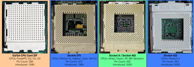
| G3/G4 ZIF | Power PC G3 G4 | 288 | 1996 |
| Socket 370 | Pentium 3, Celeron, Cyrix, Via C3 | 370 | 1999 |
| Socket A/Socket 462 | AMD Athlon, Duron, MP, Sempron | 462 | 2000 |
| Socket 423 | Pentium 4 | 423 | 2000 |
- Socket 370 – the most common socket for Intel processors. It is with this that the era of dividing Intel processors into inexpensive Celeron solutions with a trimmed cache and Pentium – more expensive full versions of the company’s product – begins. The connector was installed on motherboards with a system bus from 60 to 133 MHz. The socket is made in the form of a square plastic movable box; when installing a processor with 370 contacts, a special plastic lever presses the processor legs to the connector contacts. Supported processors Intel Celeron Coppermine, Intel Celeron Tualatin, Intel Celeron Mendocino, Intel Pentium Tualatin, Intel Pentium Coppermine. Speed characteristics of installed processors from 300 to 1400 MHz. Supported third party processors. Produced since 1999.
- Socket 423 – the first connector for Pentium 4 processors. It had a 423-pin grid of legs and was used on motherboards of personal computers. It existed for less than a year, due to the inability of the processor to further increase in frequency, the processor could not pass the frequency of 2 GHz. Replaced by Socket 478 connector. Production began in 2000.

| Type | Purpose | Number of contacts | Year of issue |
| Socket 478 / Socket N / Socket P | Intel 486 | 238 | 1994 |
| Socket 495/MicroPGA 2 | Mobile Celeron/Pentium 3 | 495 | 2000 |
| PAC 418 | Intel Itanium | 418 | 2001 |
| Socket 603 | Intel Xeon | 603 | 2001 |
| PAC 611 / Socket 700 / mPGA 700 | Intel Itanium 2, HP8800, 8900 | 611 | 2002 |
- Socket 478 - released in pursuit of the competitor (AMD company) Socket A, since previous processors were unable to raise the bar of 2 Gigahertz, and AMD took the lead in the processor production market. The connector supports Intel solutions - Intel Pentium 4, Intel Celeron, Celeron D, Intel Pentium 4 Extreme Edition. Speed characteristics from 1400 MHz to 3.4 GHz. Produced since 2000.

| Type | Purpose | Number of contacts | Year of issue |
| Socket 604/S1 | Intel 486 | 238 | 2002 |
| Socket 754 | Athlon 64, Sempron, Turion 64 | 754 | 2003 |
| Socket 940 | Opteron 2, Athon 64FX | 940 | 2003 |
| Socket 479/mPGA479M | Pentium M, Celeron M, Via C7-M | 479 | 2003 |
| Socket 478v2/mPGA478C | Pentium4, Pentium Mobile, Celeron, Core | 478 | 2003 |
- Socket 754 was developed specifically for the Athlon 64 processor. The release of new processor sockets was associated with the need to replace the Athlon XP processor line, which was based on Socket A. The first processors of AMD K8 platforms were installed in Socket 754 processor sockets measuring 4 by 4 centimeters. This need was dictated by the fact that the Athlon 64 processors had a new bus and integrated memory controllers. The voltage output from this socket was 1.5 volts. Of course, the 754 became an intermediate stage in the development of the Athlon 64. The high cost and initial shortage of these processors did not make this platform very popular. And by the time the availability and cost of components had just returned to normal, AMD presented the release of a new socket - Socket 939. By the way, it was he who helped make the Athlon 64 a popular and truly affordable processor.

| Type | Purpose | Number of contacts | Year of issue |
| Socket 939 | Intel 486 | 939 | 2004 |
| LGA 775/Socket T | Pentium4, Celeron D, Core 2, Xeon | 775 | 2004 |
| Socket 563 / Socket A / Compact | Mobile Athon XP-M | 563 | 2004 |
| Socket M/mPGA478MT | Celeron, Core, Core 2 | 478 | 2006 |
| LGA771/Socket J | Xeon | 771 | 2006 |
- Socket 775 or Socket T - the first connector for Intel processors without sockets, made in a square form factor with protruding contacts. The processor was installed on the protruding contacts, the pressure plate was lowered, and using a lever it was pressed against the contacts. Still used in many personal computers. Designed to work with almost all fourth generation Intel processors - Pentium 4, Pentium 4 Extreme Edition, Celeron D, Pentium Dual-Core, Pentium D, Core 2 Quad, Core 2 Duo and Xeon series processors. Produced since 2004. Speed characteristics of installed processors range from 1400 MHz to 3800 MHz.
- Socket 939 , containing 939 contacts with an extremely small diameter, making them quite soft. This is a "simplified" version of the previous Socket 940, usually used in high-performance computers and servers. The absence of one hole in the socket did not make it possible to install more expensive processors into it. This connector was considered very successful for its time, as it combined good opportunities, the presence of dual-channel memory access and the low cost of both the socket itself and the controller in computer motherboards. These connectors were used for computers with conventional DDR memory. Immediately after the transition to DDR2 memory, they became obsolete and gave way to AM2 connectors. The next step is invention new memory DDR3 and new AM2+ and AM3 sockets designed for the following models of AMD quad-core processors.
Socket A. This connector is known as Socket 462 and is a socket for processors from Athlon Thunderbird to Athlon XP/MP 3200+, as well as for AMD processors such as Sempron and Duron. The design is made in the form of a ZIF socket with 453 working contacts (9 contacts are blocked, but despite this, the number 462 is used in the name). The system bus for Sempron, XP Athlon has a frequency of 133 MHz, 166 MHz and 200 MHz. The weight of coolers for Socket A, recommended by AMD, should not exceed 300 grams. Using heavier coolers may lead to mechanical damage and even lead to failure of the processor power system. Processors with a frequency of 600 MHz (for example, Duron) and up to 2300 MHz (meaning the Athlon XP 3400+, which never went on sale) are supported.

| Type | Purpose | Number of contacts | Year of issue |
| Socket S1 | Athon Mobile, Sempron, Turion 64/X2 | 638 | 2006 |
| Socket AM2/AM2+ | Athon 64/FX/FX2, Sempron, Phenom | 940 | 2007 |
| Socket F/ Socket L/Socket 1207FX | Athon 64FX, Opteron | 1207 | 2006 |
| Socket/LGA 1366 | ,Xeon | 1366 | 2008 |
| rPGA988A/Socket Q1 | Core i3/i5/i7, Pentium, Celeron | 988 | 2009 |
- Socket AM2 (Socket M2), developed by AMD for certain types of desktop processors (Athlon-LE, Athlon 64, Athlon 64 FX, Athlon 64 X2, Sempron-LE and Sempron, Phenom X4 and Phenom X3, Opteron). It replaced Socket 939 and 754 connectors. Despite the fact that Socket M2 has 940 pins, this socket is not compatible with Socket 940, since more old version Socket 940 cannot support dual-channel DDR2 RAM. The first processors to support Socket AM2 were single-core models Orleans (or the 64th Athlon) and Manila (Sempron), some dual-core Windsor (for example, Athlon 64, X2 FX) and Brisbane (AthlonX2 and Athlon 64X2). In addition, Socket AM2 includes Socket F, designed for servers, and a Socket S1 variant for various mobile computers. Socket AM2+ i is absolutely identical in appearance to the previous one, the only difference is the support for processors with Agena and Toliman cores.
LGA 1366 socket – Made in 1366 contact form, produced since 2008. Supports Intel processors – Core i7 series 9xx, Xeon series 35xx to 56xx, Celeron P1053. WITH speed characteristics from 1600 MHz to 3500 MHz. Core i7 and Xeon (35xx, 36xx, 55xx, 56xx series) with integrated three-channel memory controller and QuickPath connection. Replacement of Socket T and Socket J (2008)
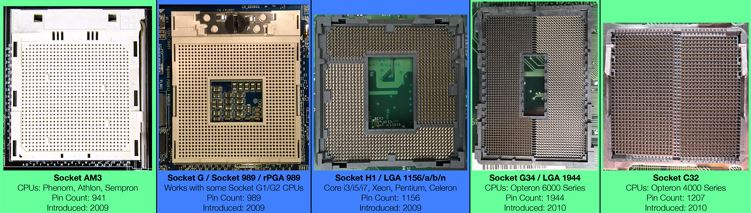
| Type | Purpose | Number of contacts | Year of issue |
| Socket AM3 | AMD Phenom, athlon, Sempron | 941 | 2009 |
| Socket G/989/rPGA | G1/G2 | 989 | 2009 |
| Socket H1/LGA1156/a/b/n | Core i3/i5/i7, Pentium, Celeron, Xeon | 1156 | 2009 |
| Socket G34/LGA 1944 | Opteron 6000 series | 1944 | 2010 |
| Socket C32 | Opteron 4000 series | 1207 | 2010 |
- LGA 1156 socket – Made using 1156 protruding contacts. Produced since 2009. Designed for modern Intel processors for personal computers. Speed characteristics from 2.1 GHz and higher.

| Type | Purpose | Number of contacts | Year of issue |
| LGA 1248 | Intel Itanium 9300/9600 | 1248 | 2010 |
| Socket LS/LGA 1567 | Intel Xeon 6500/7500 | 1567 | 2010 |
| Socket H2/LGA 1155 | Intel Sandy Bridge, Ivy Bridge | 1155 | 2011 |
| LGA 2011/Socket R | Intel Core i7, Xeon | 2011 | 2011 |
| Socket G2/rPGA988B | Intel Core i3/i5/i7 | 988 | 2011 |
- LGA 1155 socket or Socket H2 - designed to replace the LGA 1156 socket. Supports the latest Sandy Bridge processor and the future Ivy Bridge. The connector is made in 1155-pin design. Produced since 2011. Speed characteristics up to 20 GB/s.
- Socket R (LGA2011) - Core i7 and Xeon with integrated quad-channel memory controller and two QuickPath connections. Replacement Socket B (LGA1366)

| Type | Purpose | Number of contacts | Year of issue |
| Socket FM1 | AMD Liano/Athlon3 | 905 | 2011 |
| Socket AM3 | AMD Phenom/Athlon/Semron | 941 | 2011 |
| Socket AM3+ | Amd Phenom 2 Athlon 2 / Opteron 3000 | 942 | 2011 |
| Socket G2/rPGA989B | Intel Core i3/i5/i7, Celeron | 989 | 2011 |
| Socket FS1 | AMD Liano/Trinity/Richard | 722 | 2011 |
- Socket FM1 is AMD's platform for Llano processors and looks like a tempting proposition for those who love integrated systems.
Socket AM3 is a processor socket for a desktop processor, which is a further development of the Socket AM2+ model. This connector has support for DDR3 memory, as well as more high speeds HyperTransport bus operation. The first processors to use this socket were the Phenom II X3 710-20 and Phenom II X4 models 805, 910 and 810.
Socket AM3 + (Socket 942) is a modification of Socket AM3, developed for processors codenamed “Zambezi” (microarchitecture - Bulldozer). Some socket AM3 motherboards will allow you to update the BIOS to use socket AM3+ processors. But when using AM3+ processors on AM3 motherboards, it may not be possible to obtain data from the temperature sensor on the processor. Also, the power saving mode may not work due to lack of support fast switching core voltage in Socket AM3 version. The AM3+ socket on motherboards is black, while the AM3 is white. The diameter of the holes for the pins of processors with Socket AM3 + exceeds the diameter of the holes for the pins of processors with Socket AM3 - 0.51 mm versus the previous 0.45 mm.

| Type | Purpose | Number of contacts | Year of issue |
| LGA 1356/Socket B2 | Intel Sandy Bridge | 1356 | 2012 |
| Socket FM2 | AMD Trinity/athlon X2/X4 | 904 | 2012 |
| Socket H3/LGA 1150 | Intel Haswell/Broadwell | 1150 | 2013 |
| Socket G3/rPGA 946B/947 | Intel Haswell/Broadwell | 947 | 2013 |
| Socket FM2/FM2b | AMD Kaveri/Godvari | 906 | 2014 |
- Socket H3 or LGA 1150 is a processor socket for Intel processors of the Haswell (and its successor Broadwell) microarchitecture, released in 2013. LGA 1150 is designed as a replacement for LGA 1155 (Socket H2). Made using LGA (Land Grid Array) technology. It is a connector with spring-loaded or soft contacts, to which the processor is pressed using a special holder with a grip and a lever. Officially confirmed that LGA 1150 socket will be used with sets Intel chips Q85, Q87, H87, Z87, B85. The mounting holes for cooling systems on sockets 1150/1155/1156 are completely identical, which means full comprehensive compatibility and identical installation procedures for cooling systems for these sockets.
- Socket B2 (LGA1356) - Core i7 and Xeon with integrated three-channel memory controller and QuickPath connections. Replacement Socket B (LGA1366)
- FM2 connector - Processor socket for hybrid processors (APU) from AMD with the Piledriver core architecture: Trinity and Komodo, as well as the canceled Sepang and Terramar (MCM - multi-chip module). Structurally, it is a ZIF connector with 904 pins, which is designed for installing processors in PGA-type cases. The FM2 connector was introduced in 2012, just a year after the FM1 connector. Although socket FM2 is an evolution of socket FM1, it is not backward compatible with it. Trinity processors have up to 4 cores, Komodo and Sepang server chips have up to 10, and Terramar have up to 20 cores.

| Type | Purpose | Number of contacts | Year of issue |
| LGA 2011-3 / LGA 2011 v3 | Intel Haswell, haswell-EP | 2011 | 2014 |
| Socket AM1/FS1b | AMD Athlon/Semron | 721 | 2014 |
| LGA 2011-3 | Intel Haswell / Xeon / haswell-EP / ivy Bridge EX | 2083 | 2014 |
| LGA 1151/Socket H4 | Intel Skylake | 1151 | 2015 |
- LGA 1151 socket - a socket for Intel processors that supports Skylake architecture processors. LGA 1151 is designed as a replacement for LGA 1150 (also known as Socket H3). LGA 1151 has 1151 spring-loaded contacts to contact the processor pads. According to rumors and leaked Intel advertising documentation, motherboards with this socket will feature DDR4 memory support. All Skylake architecture chipsets support Intel Rapid Storage Technology, Intel Clear Video Technology and Intel Wireless Display Technology (when supported by the processor). Most motherboards support various video outputs (VGA, DVI or - depending on the model).


| Type | Purpose | Number of contacts | Year of issue |
| LGA 2066 Socket R4 | Intel Skylake-X/Kabylake-X i3/i5/i7 | 2066 | 2017 |
| Socket TR4 | AMD Ryzen Threadripper | 4094 | 2017 |
| Socket AM4 | AMD Ryzen 3/5/7 | 1331 | 2017 |
- LGA 2066 (Socket R4) - a socket for Intel processors that supports processors Skylake-X architecture and Kaby Lake-X without an integrated graphics core. Designed to replace the LGA 2011/2011-3 (Socket R/R3) socket for high-end Basin Falls desktops (X299 chipset), while the LGA 3647 (Socket P) will replace the LGA 2011-1/2011- 3 (Socket R2/R3) in server platforms based on Skylake-EX (Xeon “Purley”).
- AM4 (PGA or µOPGA1331) is a socket produced by AMD for microprocessors with Zen microarchitecture (Ryzen brand) and subsequent ones. The connector is a PGA (pin grid array) type and has 1331 contacts. It will be the company's first socket with support for the DDR4 memory standard and will be a single socket for both high-performance processors without an integrated video core (currently using Socket AM3+), and for low-cost processors and APUs (previously using various sockets of the AM / FM series).
- Socket TR4 (Socket Ryzen Threadripper 4, also Socket SP3r2) is a type of connector from AMD for the Ryzen Threadripper family of microprocessors, introduced on August 10, 2017. Physically very close to the AMD Socket SP3 server connector, however, it is incompatible with it. Socket TR4 became the first LGA-type socket for consumer products (previously LGA was used in the server segment, and processors for home computers were produced in FC-PGA packages). It uses a complex multi-stage process of mounting the processor into the socket using special holding frames: an internal one, secured with latches to the cover of the chip case, and an external one, secured with screws to the socket. Journalists note the very large physical size of the connector and socket, calling it the largest format for consumer processors. Due to its size, it requires specialized cooling systems that can handle up to 180W. The socket supports HEDT (High-End Desktop) segment processors with 8-16 cores and provides the ability to connect RAM via 4 DDR4 SDRAM channels. The socket has 64 generation 3 PCIexpress lanes (4 are used for the chipset), several 3.1 and SATA channels
Leave your comment!